現在、インターネットにつながるモノ(IoT)の数は爆発的に増加しています。持続可能なIoT社会を実現するためには、安価で環境に配慮したフレキシブルデバイス作製技術が必要不可欠となります。本研究では、レアメタルを極力使用せず、豊富で安価な材料のみを用いて作製できる半導体成膜技術、キャリア制御技術、さらにフレキシブルなプラスチックフィルム等に機能性薄膜を形成できる技術により、新たなIoTフレキシブルデバイス集積化技術の創出を目指しています。
The number of Internet-connected devices (IoT) is currently increasing exponentially. To realize a sustainable IoT society, affordable and environmentally conscious flexible device fabrication technology is essential. This research aims to create new IoT flexible device integration technology. This will be achieved through semiconductor film deposition techniques that minimize the use of rare metals, employing only abundant and inexpensive materials; carrier control technology; and techniques enabling the formation of functional thin films on flexible substrates such as plastic films.
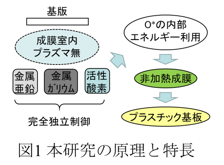
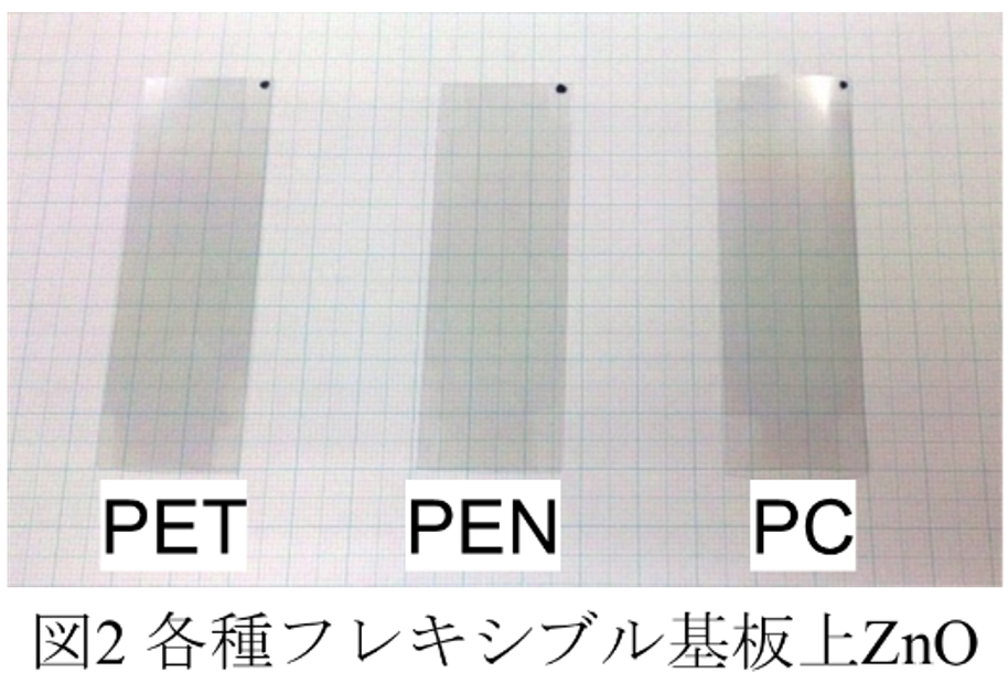
シリコンに代表される従来の半導体成膜形成手法では、薄膜形成時およびデバイス作製時に高温での熱処理が必要となり、プラスチックなどの耐熱性のないフレキシブル基板への形成が困難でした。本研究室ではこの課題を克服するため、分子線エピタキシー(MBE)法および原子状酸素ラジカルを利用した独自の酸化亜鉛(ZnO)系薄膜の低温形成手法の開発とそのデバイス応用に取り組んできました。酸素ラジカルの高い反応性を利用してZnO薄膜を形成するため、酸素と亜鉛を反応させるのに必要なエネルギーを基板から熱エネルギーとして与える必要がなく、非加熱成膜が可能になり(図1)、耐熱性の低い各種プラスチック基板にも対応できます(図2)。
Conventional semiconductor thin-film deposition methods, such as those using silicon, require high-temperature heat treatment during thin-film formation and device fabrication. This made it difficult to form films on flexible substrates like plastics, which lack heat resistance. To overcome this challenge, our laboratory has focused on developing a unique low-temperature formation method for zinc oxide (ZnO) thin films using molecular beam epitaxy (MBE) and atomic oxygen radicals, along with its device applications. By utilizing the high reactivity of oxygen radicals to form ZnO thin films, the energy required to react oxygen and zinc does not need to be supplied as thermal energy from the substrate. This enables non-heated film formation (Fig. 1) and allows compatibility with various low-heat-resistant plastic substrates (Fig. 2).
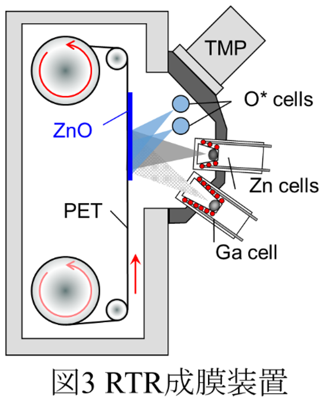
この手法により、ZnOにガリウムを添加したGZO透明導電膜の形成や、トランジスタ応用可能な100nm以下のチャネル層を有するZnO極薄膜の開発に成功しています。低温および低損傷プロセスであるため、PETやPENなどの各種プラスチック基板にRoll to Roll(RTR)方式(図3)で導電膜、半導体薄膜、絶縁膜を一体かつ連続成膜することが可能であり、従来の半導体基板とは異なる安価な大面積フレキシブル基板上に次世代デバイスを実現する可能性を有しています。
This technique has enabled the formation of GZO transparent conductive films by adding gallium to ZnO, as well as the development of ultra-thin ZnO films with channel layers below 100 nm suitable for transistor applications. Because it is a low-temperature and low-damage process, it enables the integrated and continuous deposition of conductive films, semiconductor thin films, and insulating films onto various plastic substrates such as PET and PEN using a Roll-to-Roll (RTR) method (Fig. 3). This holds the potential to realize next-generation devices on inexpensive, large-area flexible substrates, differing from conventional semiconductor substrates.