
希薄磁性(微量な磁性元素を含んだ)半導体を用いて電子が持つ電荷とスピンの両方を工学的に利用する『スピントロニクス』の実現を目指します。セレン化亜鉛(ZnSe)を用いた希薄磁性半導体ナノ構造においては、スピン効果と励起子効果が顕著に現れます。これらの性質を利用した新しい原理の信号伝送を実現するデバイスの開発に取り組んでいます。
We aim to realize ‘spintronics’—the engineering utilization of both the charge and spin of electrons—using dilute magnetic semiconductors. In dilute magnetic semiconductor nanostructures using zinc selenide (ZnSe), both spin effects and exciton effects are prominently observed. We are developing devices that realize novel signal transmission principles utilizing these properties.
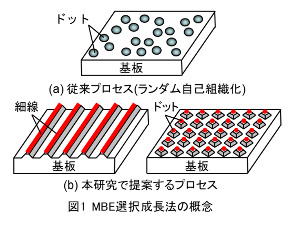
本研究の特徴は、分子線エピタキシー(MBE)選択成長法により、図1に示すような量子集積回路の基本構造を一度に大面積に形成する点にあります。
A key feature of this research is the ability to simultaneously form the fundamental structure of quantum integrated circuits, as shown in Fig. 1, over a large area using molecular beam epitaxy (MBE) selective growth.
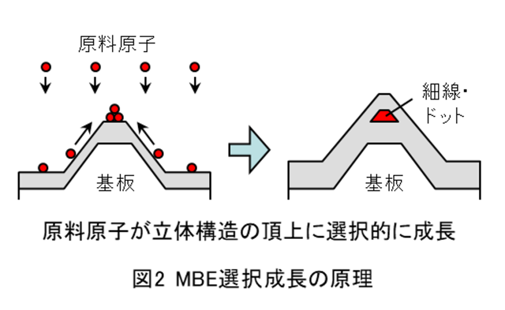
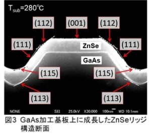
この手法は、リソグラフィー技術と化学エッチングによって微細な立体加工を施した半導体基板上へ、高純度な原料を分子(原子)線状に照射することにより、図2に示すような原子レベルの構造を自己組織化する方法で、従来のプロセスにおいて問題となっていたランダムにしか形成できないナノ構造の位置制御に関する弱点を克服することが可能になります(図3)。
This method involves irradiating high-purity raw materials in a molecular (atomic) beam onto a semiconductor substrate that has undergone fine three-dimensional processing via lithography and chemical etching. This enables the self-assembly of atomic-level structures, as shown in Figure 2. It overcomes the weakness in conventional processes where nanostructures could only be formed randomly, addressing the challenge of positional control (Fig. 3).
本研究では、この手法をさらに発展させ、単に微細な構造を形成するだけでなく、あらかじめ基板上でこれらの構造を有機的に連結させたパターンを設計することでネットワーク状の回路を構築し、新たな集積光電子デバイスへ応用することを目標としています。
This research aims to further develop this technique, not only to form fine structures but also to construct networked circuits by designing patterns that organically interconnect these structures on substrates in advance, with the goal of applying them to novel integrated optoelectronic devices.
この手法により、高品質なナノ構造の自己組織化プロセスが確立されれば、結晶工学などの基礎学問分野への貢献はもとより、半導体電子デバイス・光デバイス工学といった応用工学分野への多大な貢献が期待できます。また、正確な位置およびサイズ制御性から、従来から使用されてきた信頼性の高い素子・回路設計技術の適用が可能となるため、他のナノ構造作製手法に比べ生産プロセスとしての拡張性に優れています。本研究は、量子効果デバイスによる新たな集積回路の実現に向けて独創的な手法で取り組むものであり、研究達成時には、次世代情報技術を取り巻く関連分野へ大きな波及効果が期待できます。
This approach, if it establishes a self-organization process for high-quality nanostructures, is expected to contribute significantly not only to fundamental academic fields such as crystal engineering but also to applied engineering fields like semiconductor electronic device and optical device engineering. Furthermore, its precise position and size controllability enables the application of established, reliable device and circuit design technologies, making it superior in scalability as a production process compared to other nanostructure fabrication methods. This research pursues innovative approaches toward realizing new integrated circuits using quantum effect devices. Upon successful completion, it is anticipated to have substantial ripple effects across related fields surrounding next-generation information technology.